

Building Glitchy: an open-source hardware hacking tool
Power glitching to bypass instruction flow and power monitoring to interrogate program branching. Or in other words, glitch it to bypass that password check or power monitor it to recover that password.
- Open source hardware and software project! Click the PROJECT REPO button at the top to see it. There’s also a Wiki to walk you through some beginning lessons.
- Funded by and developed for a client to use with their internal red team and at hacking events.
- Biggest tech challenge: making an ESP32 consistently produce 18 ns pulses
- Designed as an introductory learning tool, and to be as cheap and simple as possible. We’re not competing with ChipWhisperer or any other professional tools here.
- Uses real third-party hardware for targets, not special-built boards designed to be exploited.
So why Glitchy? There’s tools out there already that do this stuff and more. When I was approached by a friend about this project, they needed something that lowered the barrier to exploring hardware security exploitation. They wanted something that was cheap enough to hand out like badges at conferences and was geared toward beginners in the hardware hacking area. The vision was to use it with a client’s internal red team, experts in software attacks on CPU architectures, and help them explore the hardware aspect aka side channel attacks. We also agreed to open source this project so others could learn from it, which I was ecstatic about. Most of the work I do gets buried behind NDAs never to see the light of day, and I can actually share this one with you.
So where to start? I like looking at the trade space. There’s a thousand ways to make this thing, so how do we choose? Since it was open source, I wanted the hardware and software to be as accessible as possible — so that’s where I began.
PCB
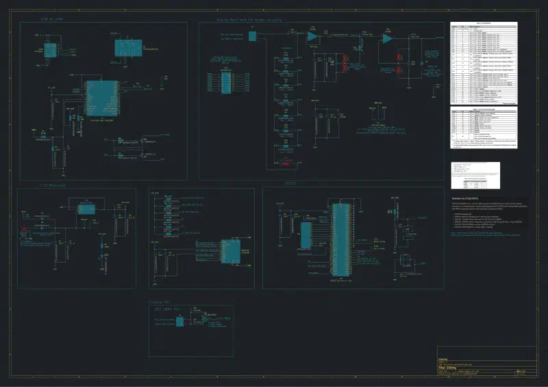
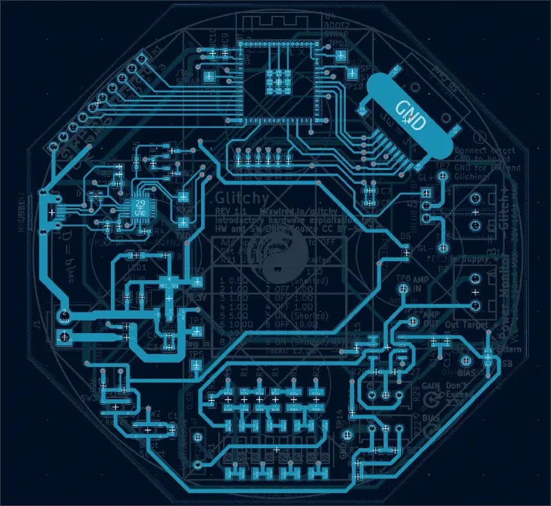
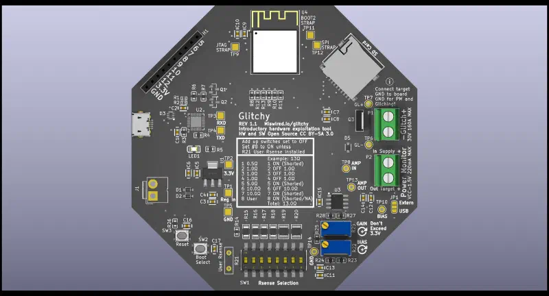
What should I design the PCB in? I am good in Altium, but unless you are a professional, chances are you can’t afford that. So I built it in KiCad. It’s free and it’s what most hobbyists use. Honestly KiCad has gotten really good over the years and I enjoy using it over Altium for basic projects.

The Brains
What should we run this on? I am a huge fan of Cypress PSoC chips (acquired by Infineon in 2019). The analog front end would have made this project SUPER easy. But beginners know Arduinos and ESP32s. So I took the challenge to see if I could get the performance out of an ESP32. It was cheap and it’s got Wi-Fi and can host basic webpages for control.
This turned into a whole journey I had no idea was coming. So many debugging hours and drilling down through datasheets. The ESP32 chips make this challenging for two reasons.
- To do power glitching, we need to very quickly and very accurately toggle IO lines
- To do power monitoring, we need low noise and decently fast analog to digital (ADC) functionality
Power Glitching
The concept of power glitching is surprisingly simple, while its execution is difficult to accomplish. In power glitching what you want to do is short the power supply to a chip just long enough that it misbehaves, but not so long it resets. That’s basically it. Do it just hard enough, just long enough, at just the right time, and that if statement that was supposed to come back and say “no you don’t have the right password” malfunctions and says “yup, you are good to go!”.
Source: Target_keypad.ino — the demo target’s password check, from the project repo (Code/Target Examples/Target_keypad/).
// g_was_the_right_key_pressed is declared volatile so the compiler can't
// optimize it away or assume its value. It is initialized false and never set
// true in normal execution, so this branch should never be taken -- until a
// glitch corrupts the check.
volatile bool g_was_the_right_key_pressed = false;

//Check to see if button is pressed and we should evaluate the password
if (!digitalRead(ENTER_KEY_PIN)) {
  Serial.println("Enter Key Pressed\n");
  if(g_was_the_right_key_pressed)
  {
    unlock_system();
  }
}if, calling unlock_system() even when the wrong key was pressed.The circuit for power glitching is also very simple. It’s a Field Effect Transistor (FET) that is connected between the power and ground rails of the target, and it’s turned on very quickly, for a brief moment. In the world of side channel attacks, this FET is often called the crowbar FET. Activate it too long and you just turn the chip completely off, resetting it, or trip the brown out detector and it resets it for you. Too short and nothing happens.
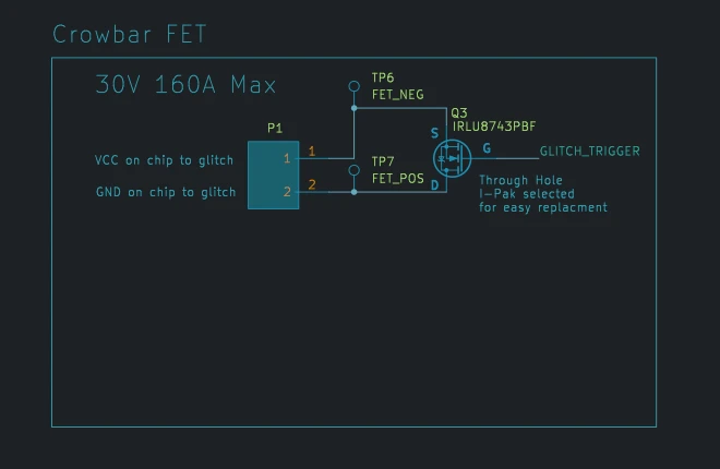
Not only is it a fine balance to achieve — it also has to be done at exactly the right time. That means it often takes very short pulses on the order of nanoseconds, or 0.000000001 s, to drive the crowbar FET just enough to hit that balance point.
Boy did I set myself up for a challenge picking the ESP32 for this. I ran into the most frustrating random behavior trying to get repeatable glitching pulses. I started by doing a quick back of the napkin calculation to see what was theoretically possible with the chip. (Wrongly, it turns out.)
Breaking down the theory, I looked at the ESP32-S3-MINI-1-N8 module’s datasheet and saw it had a 240 MHz clock, and this processor typically can complete one simple instruction per clock cycle. I made a gross assumption that if I wrote optimized assembly, I could theoretically send two commands, IO high and IO low back to back. Optimistically that might be two clock cycles, so maybe 240 MHz / 2 = 120 MHz, or 1/120 MHz = 8.3 ns. That’s not bad! Knowing there were probably other practical limitations here, that number was enough for me to spend a couple bucks getting one to see what I could actually get from it.
However, after lots of code optimization, reading datasheets, controlling the IO registers directly, I discovered the best I could get from it was 40 MHz or 25 ns. And that was with hand optimized assembly, and it wasn’t consistent. I had missed that the IO bus runs on its own 80 MHz clock. But more than that, it was constantly being interrupted and even with interrupts off, I would get random pulses that were hundreds of ns and then jump back to 25 ns. Sometimes it would behave for hours and then the next day, I couldn’t get any pulses shorter than 100 ns. It was maddeningly inconsistent.
On top of that, the duration of the pulse isn’t the only thing to consider, you also have to trigger that pulse at an exact time. And there was so much jitter (variance) between the trigger and when the pulse happened, it was looking like this would never work.
Then I had a clever idea that solved everything! Like most microcontrollers the ESP32 has specialized hardware for communications lines. Things like serial, I2C, and SPI, and they often have their own clocks and dedicated logic so the CPU jitter doesn’t affect the communications. I knew pulses from these modules would be clean and repeatable and not prone to the CPU interrupts. But could I change the pulse lengths and reliably trigger them?
More digging I found the SPI module has clock scaling. Testing the module I was getting rock solid 18 ns pulses on the oscilloscope! It should have theoretically been 12.5 ns. I attributed the extra time to a combination of capacitive loading and internal shift register delays from the SPI module. So I wrote a function to adjust the timing by changing the clock scaling. Note the function below isn’t perfect, there are discrete time steps, it just tries to get as close to the requested time as possible. But it is stable, repeatable, and it works!
Source: glitching.cpp — the function that fires the pulse, from the project repo (Code/Glitchy/src/).
//Shortest time about 18ns, longest time about 10000ns
void execute_spi_driven_glitch(unsigned long time_ns)
{
  unsigned long drive_frequency = 1/(0.000000001 * time_ns);

  spi_fspi.beginTransaction(SPISettings(drive_frequency, MSBFIRST, SPI_MODE0));
  spi_fspi.transfer(0b00000001);
  spi_fspi.endTransaction();
}While I don’t have any screenshots of the raw IO out, I can show you what a successful power glitch on an Arduino looks like. This is the VCC (Power) line to the Arduino.
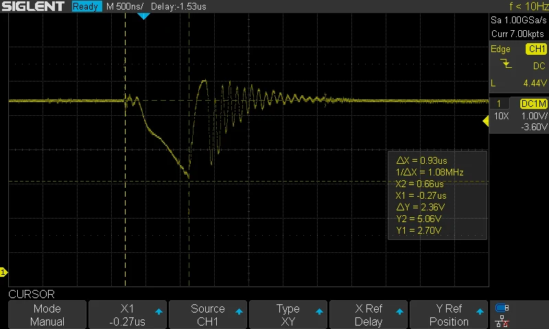
Here we used a glitch pulse of about 0.93 µs, which crowbars the supply down from ~5.06 V to ~2.70 V. The goal is to disrupt a single instruction — though it’s not an exact science: internal capacitance, drain time, and other variables mean you may corrupt more than you intend. Either way, it’s short enough not to reset the chip. You can read more about the methodology and walk through the class lab in the wiki at the repo link at the top of this article. But basically, you trigger an event, and try several times at varying glitch pulse widths until you get the result you want.
This successfully bypassed the if check in the example code we included above, something that can only be done by glitching.
Power Monitoring
The other challenge going into this was knowing the ESP32’s analog-to-digital (ADC) conversion was very noisy internally. I had no idea if it would be up to the task of measuring minute power differences caused by different code execution flows in something like a small microcontroller.
I started by breadboarding some different basic filters and amp design. And when I say breadboarding I don’t mean protoboarding or prototyping. I mean grabbing a breadboard with through hole components building prototype circuits out there. You can quickly switch around components and change the topology. It’s like Legos with circuits.
Back to the ADC front end design. My thought was, if I make the signal large enough, and I drive the ADC with a solid amp, we should be able to overcome those limitations.
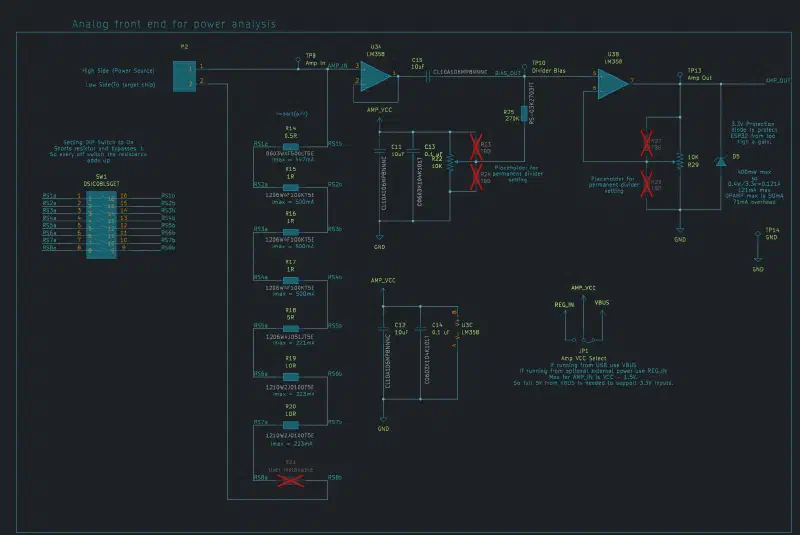
The sense resistor
Fundamentally we want to be able to sense the current going to the target. One of the ways of doing this is putting what is called a shunt or sense resistor in line with the power supply to the target. However there is a tradeoff here with the value of the resistor.
The higher the resistor, the larger the voltage signal across it develops, and the easier to sense and process it. But that voltage drop across the resistor also takes away voltage to the target, and if you take too much away, the chip will brown out and not work at all.
Too low of a resistor, and the target is perfectly happy, but you can’t read the tiny voltage signal across that resistor and you just get noise.
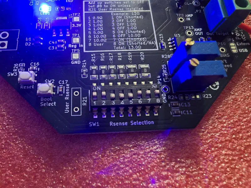
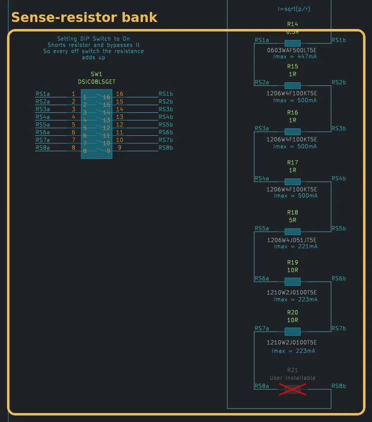
And every target is different and has different current requirements. So the first part in the circuit is a configurable sense resistor. There is a resistor chain with dip switches that short out each resistor to bypass it, allowing you to configure how much resistance to use.
Buffer Amp
One of the tradeoffs of this design for cost savings was using cheap single ended op-amps which means that the Glitchy board and the target board must share a ground. You will notice the buffer amp just has the one input to it, because it’s referencing that input to GND. Why have a buffer amp here? Put simply, op-amps in this configuration take very little current at their inputs, and use whatever power supply they’re hooked up to in order to produce a higher current mirror of the voltage signal they’re given. It’s worth noting there are MANY ways of using op-amps. What I am describing is the unity gain amplifier, or buffer amp you see here.
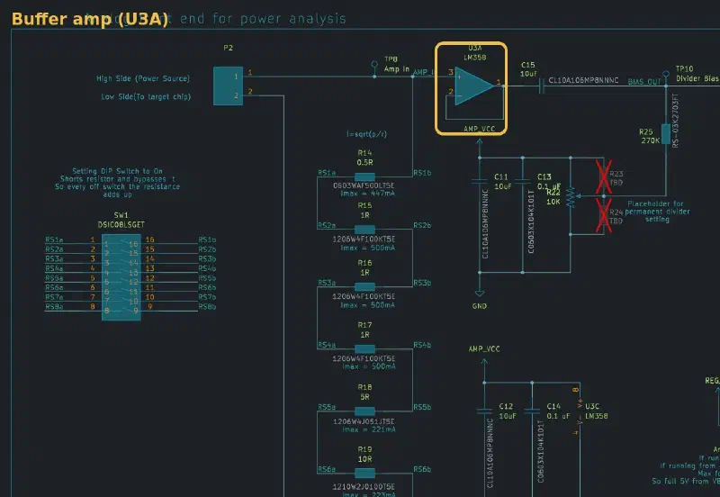
AC coupling
The job of the capacitor right after the buffer amp is to AC couple. Or in other words, we only want the CHANGE in voltage to be transmitted through, not the static DC bias. For example, say we have a 1 V steady DC voltage, and on that was riding a 1 kHz AC signal. If we only want that 1 kHz AC signal, we would AC couple it with a capacitor.
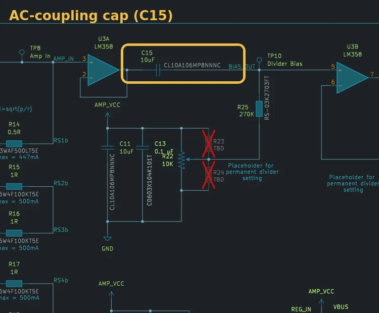
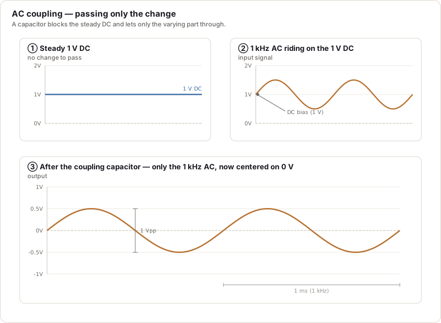
The mechanism for how this works and why and the selection of the capacitor value and type are beyond the scope of this article. I might do a series on Electrical Engineering 101 at some point that would dive deeper into that. For now you can accept the ideal case that we are getting the signal changes through.
Bias Point
The next section is a resistor divider connected to a variable resistor, called a potentiometer. Remember how I mentioned a single ended amp setup? A single ended amp can only output positive voltage within whatever its power rails are. Adding a negative voltage rail here would have cost more and made this more complex. An alternative is you can bring the signal up so any negative signal gets shifted up into a readable range.
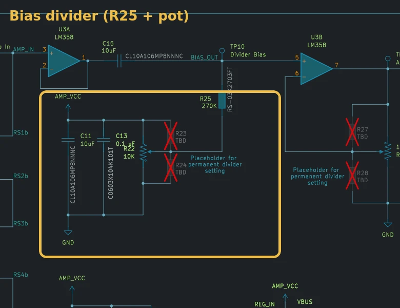
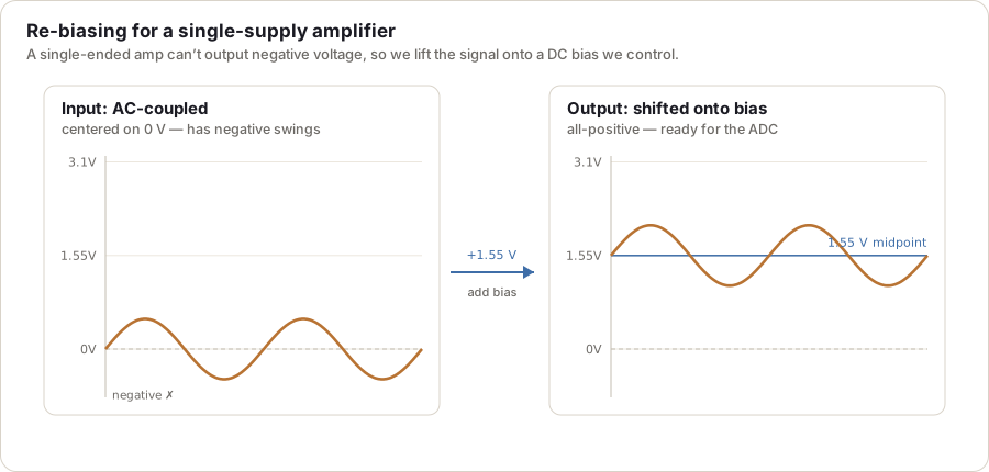
You might be asking yourself, why did we go through the trouble of removing the DC bias just to add it again? The answer here is, we get to control the DC bias, and we need to make sure it’s in a range that the ADC on our chip can actually read. It has limits on what we can put into it without damaging it, it also has performance considerations on where it operates well at. Here we get to tune that point.
You will also see the first Do Not Populate (DNP) also called Do Not Install (DNI) symbol. On the delivered board I left these as potentiometers to allow for adjustment. But it’s just as easy to DNP the potentiometers and select static resistor values if you want to constrain the tool to one current range and make it simpler for the user.
The second amp
This last op-amp performs two tasks. First, it acts as a current buffer again so whatever we connect the output of this circuit to, doesn’t affect our resistor bias point. The same job as our input buffer. Second, it has variable gain. It lets us magnify the signal coming in so that the ESP32’s ADC input can hear the signal better.
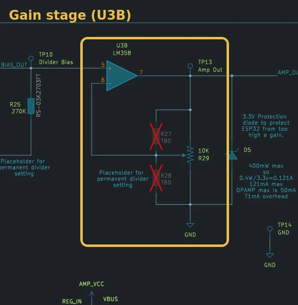
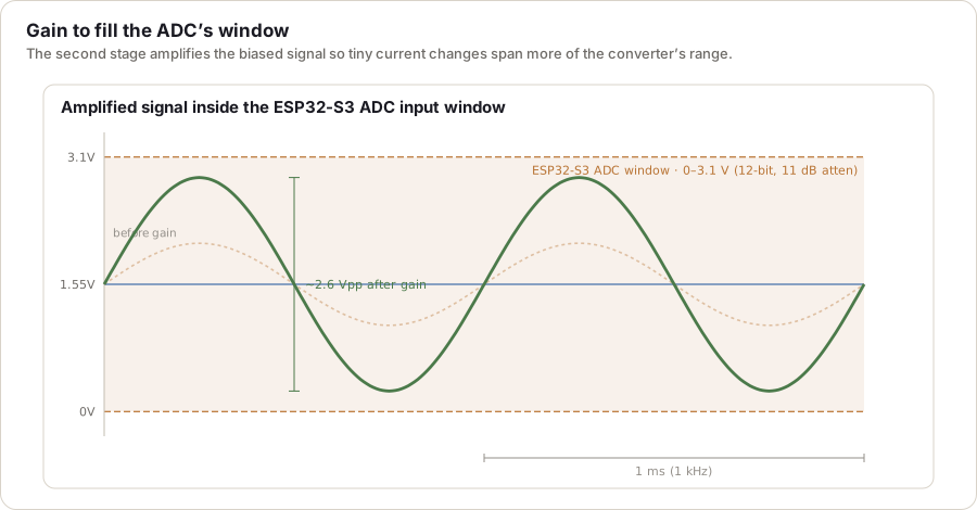
This flow lets us measure very small changes in a target’s current consumption.
The protection diode
The final part in this section of the circuit. It’s likely that people, especially people learning, are going to just turn dials and see what happens. And because we are powering the op-amps with 5 V, it’s possible to crank the gain up and exceed the ESP32’s input range, damaging the chip. So I have placed a protection diode at the output here. This is a Zener diode. Its role is to start conducting and short the signal if the voltage peaks too high, and thus protecting the ESP32.
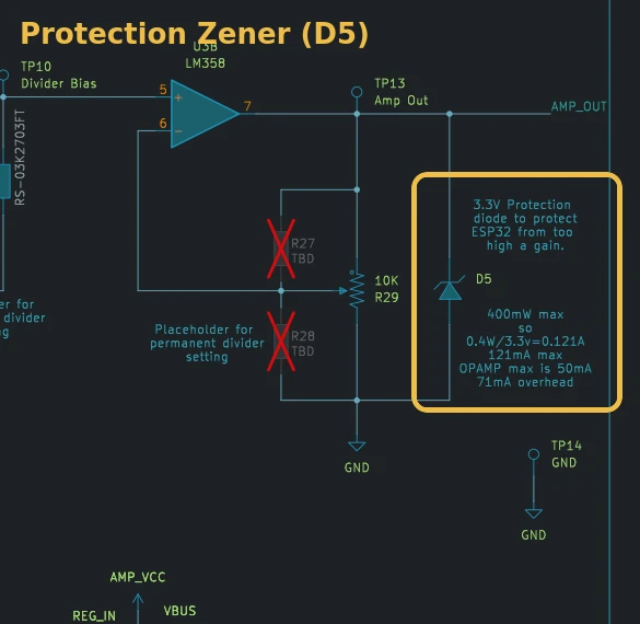
Putting it all together
All this allows us to monitor the changes in a test program on the Arduino. The demo uses three keys, one of which runs a different code path. As you press each one, it looks at the current profile right after each button press. You can clearly see which key looks different in this screenshot.
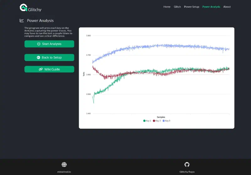
In embedded systems it is very common to check each digit of a password as it is fed into the microcontroller from a keypad. This is a vulnerability, because you are able to test each key on the first digit of the password, figure that out, then move on to the next digit, and eventually decode the combination or password. It looks like this:
- Reset the chip so you are on the first digit
- Send the number 1, capture the current
- Reset again so you are on the first digit
- Send the number 2, capture the current
- Rinse and repeat until you have tried all combinations for the first digit
- Figure out which one of the keypresses stands out for the first digit of the combination
- Reset the board, put in the first digit of the combination
- Send the number 1, capture the current
- Reset the board, put in the first digit of the combination
- Send the number 2, capture the current
- Rinse and repeat until you have done all the numbers and captured all the traces again
- Determine the second digit of the combo.
And so on…
And pretty soon you have the full combo to an electronic lock or something similar!
The demo program in the repo is pretty basic to demonstrate this point, but this is a very real vulnerability, and the same technique is also used to extract encryption keys through stochastic analysis.
The Target
Here was another point that I was adamant about. A lot of kits, even the ChipWhisperer which is arguably the leader in this area, uses special boards they designed for you to glitch and test with. It always felt to me underwhelming and disconnected from the point I want to get across.
Of course the hardware you designed is going to glitch or exploit the board you specifically designed to be glitched and exploited. Are the techniques going to work in the real world? I wanted the target for Glitchy to be something cheap that everyone is familiar with. That’s why I picked the Arduino Uno.
Below are some pictures of soldering on wires to the ATMEGA’s power bypass capacitor that feeds the chip its power.
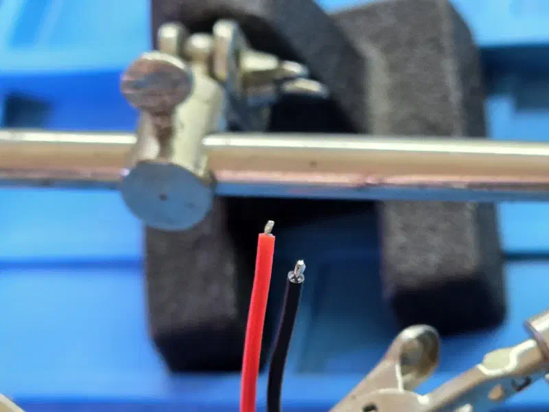
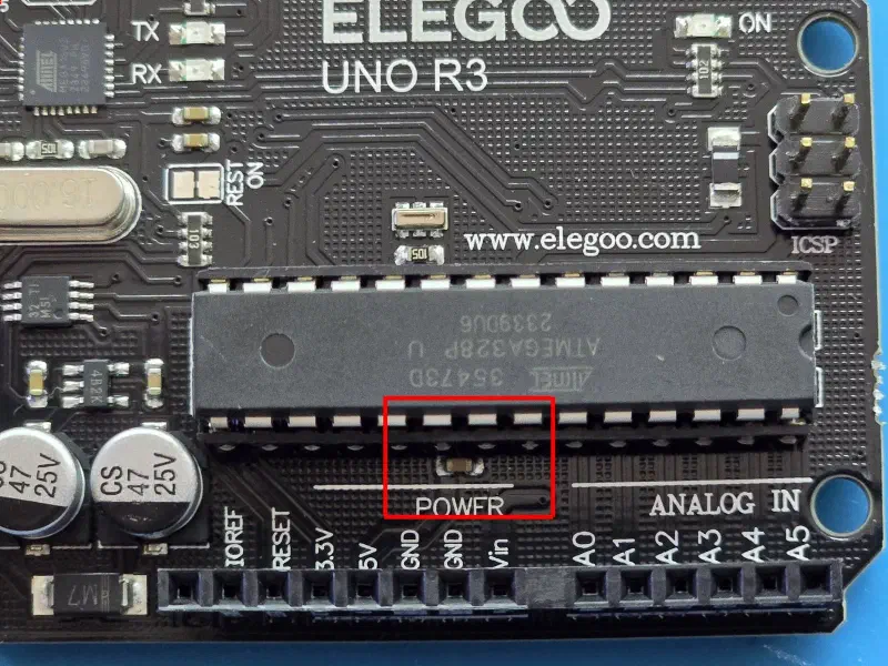
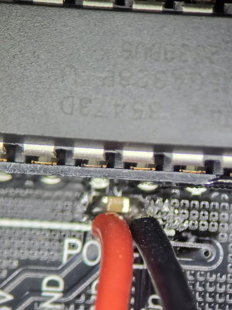
On most targets you tend to want to remove those bypass capacitors, as their job is to specifically help the chip stay up when there are power fluctuations. However, the crowbar on the Glitchy is so strong that at least for the Arduino Uno it didn’t matter so it’s easier to just leave it on.
Note we are not trying to short out the power to the Uno’s input power port before we even hit the regulator. Glitching there would be fighting all the regulator circuitry and capacitance. It would be impossible to bring the power on the microcontroller down the way we need to from that point. So we solder on as close to the target as possible. Also on real systems, we don’t want to glitch all the supporting hardware around the chip, just the target chip.
Again, there are a couple step by step lessons in the project repo with some vulnerable Arduino demo code.
Control Interface
This project runs a web interface to control the parameters and initiate the glitching. The first version of the web interface I wrote from scratch and it was very rough. This was 2024, before the current boom in AI capability. Otherwise I’d have leaned on an agent to help improve the look and review my code and design along the way. But alas this wasn’t an option, so I did the next best thing. I hired a good friend of mine that is much better at web design than I am to improve the web interface.
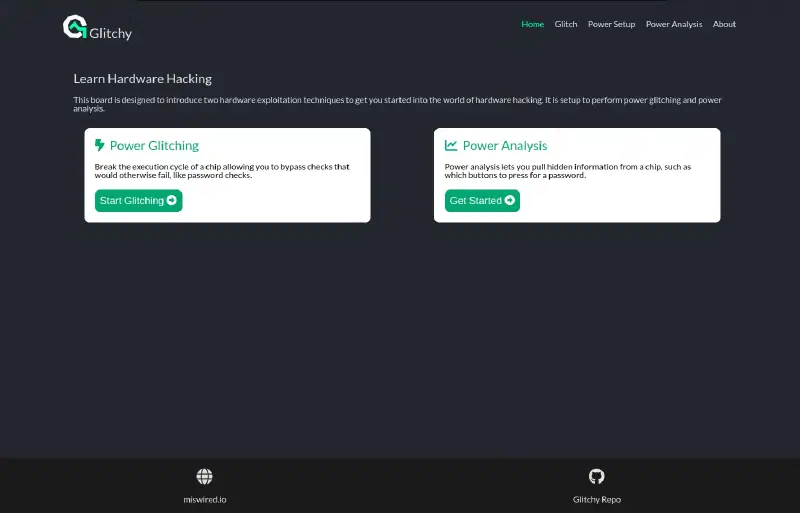
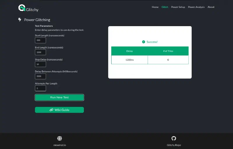
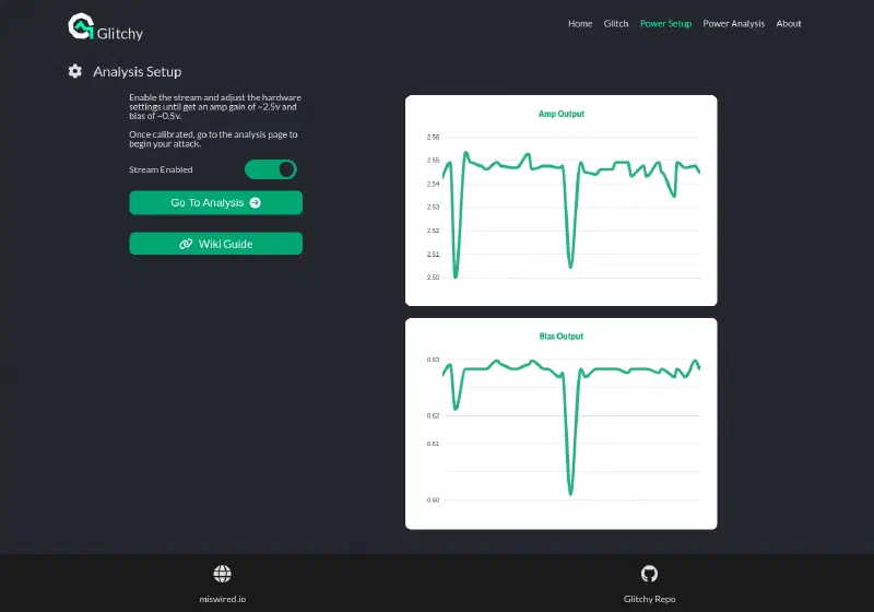
The repo for the web interface is also open source and is also linked in the project repo.
There is an additional benefit to having a wireless control interface. Things get complicated and noisy fast doing power analysis when multiple grounds and power sources are added. Being wireless means the computer doing the control is completely isolated from the target. So much improved noise profile, and you avoid ground loop issues that can completely kill your signal.
Board cost estimation
Roughly what it costs to build one, using current LCSC parts and JLCPCB for the 2-layer board. In hobby quantities the parts run about $10 a board — the ESP32-S3 module alone is nearly half of that — dropping toward $7–8 at a hundred units.
| Qty | Parts + bare PCB (you hand-solder) | + turnkey SMT assembly |
|---|---|---|
| 5 | ~$11–12 | ~$22 |
| 30 | ~$8.5 | ~$10 |
| 100 | ~$7.8 | ~$8.5 |
Prices are ballpark and exclude shipping and tax. Turnkey assembly only starts to pay off past a few dozen boards, since it carries around $50 in one-time setup and part-loading fees.
Wrapping up
So there we have it, an open-source, open-hardware gadget you can use to exploit real hardware and learn about side-channel attacks. All packed into a low cost board with some neat tricks to make the ESP32 do things it was clearly never scoped to do. My hope is that others will take this, hack on it, and learn along the way. I am very open to collaborators if anyone wants to submit a pull request.
Interested in hiring someone to do this for you? → See what I offer